A new $3.5 million award from the National Institute of Standards & Technology will help the University of Arkansas expand its research and development in the power packaging field.
Power packaging is a process in semiconductor manufacturing that protects, connects and cools the high-power chips.
“Consider the boxy plug of a cell phone charger,” a press release from the university stated. That box converts the AC electricity coming out of the wall outlet to the DC power charging the battery. The various elements inside the plug that allow it to do this are its power packaging, all of which is built around a semi-conducting material.
The $3.5 million in funds will allow the university’s High-Density Electronics Center (HIDEC) to upgrade its facility and become a Power Packaging Center of Excellence.
The release stated that as the need for power increases, whether for electric cars, planes or bulldozers, the packaging of the semiconductor technology becomes more complex as it converts and transfers more power. Advanced power packaging is essential to operating at high voltages, high currents and high temperatures. Advanced power packaging also contributes to energy efficiency, a consideration as more data centers are constructed to power AI.
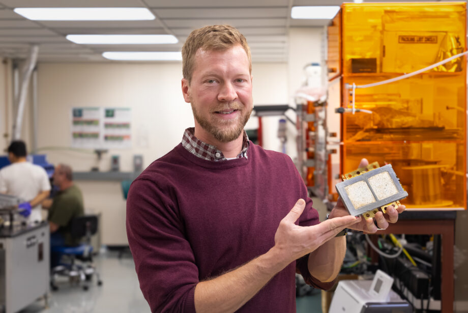
David Huitink, an associate professor of mechanical engineering and current director of HIDEC, is the principal investigator who will lead the advancement of HIDEC to an updated and expanded research center.
The funds will be used to upgrade the existing equipment used in electronics assembly and expand the lab’s capabilities to have a more complete suite of tools.
The upgrades aim to help cement the university as a leader in power packaging by providing campus researchers with state-of-the-art equipment. This will facilitate more service contracts with external partners, morel federal research funding due to increased expertise and capabilities and new intellectual property through patented technology stemming from research and development.
HIDEC is part of the UA Power Group, which brings together a range of interdisciplinary researchers to study issues related to power and energy. HIDEC will work with the recently opened Multi-User Silicon Carbide Research & Fabrication Laboratory to build power packaging around silicon carbide wafers developed and prototyped by the lab.
“We want to be the undisputed number one,” Huitink said in the release. “We’re already there in some ways, but we want to establish very clearly that the U of A is the place to come for R&D and prototyping work in wide bandgap electronics.”
U.S. Sen. John Boozman helped secure the federal appropriations for the research center.